
WASHINGTON, D.C. – The research into Graphene nanotubes continues. The opportunities that this new miracle compound presents are almost unlimited.
Carbon nanotubes’ outstanding mechanical, electrical and thermal properties make them an alluring material to electronics manufacturers. However, until recently scientists believed that growing the high density of tiny graphene cylinders needed for many microelectronics applications would be difficult.
Simple New Technique for Graphene Nanotube Forests
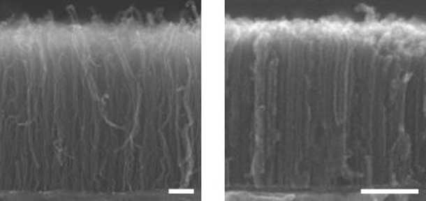
Now a team from Cambridge University in England has devised a simple technique to increase the density of nanotube forests grown on conductive supports about five times over previous methods. The high density nanotubes might one day replace some metal electronic components, leading to faster devices.
“The high density aspect is often overlooked in many carbon nanotube growth processes, and is an unusual feature of our approach,” says John Robertson, a professor in the electronic devices and materials group in the department of engineering at Cambridge. High-density forests are necessary for certain applications of carbon nanotubes, like electronic interconnects and thermal interface materials, he says.

Photo Credit: Hisashi Sugime/U.Cambridge
Graphene has a Northwestern Ontario Opportunity
The importance of the research into graphene has very large implications for Northwestern Ontario. In the region, exploration into vein carbon graphite by Zenyatta Ventures offers a massive potential supply of the core material needed for Graphene.
With concerns raised over the Ring of Fire chromite development, the ‘Ring of Graphite’ could be in the long term equally positive.
Robertson and his colleagues grew carbon nanotubes on a conductive copper surface that was coated with co-catalysts cobalt and molybdenum. In a novel approach, the researchers grew at lower temperature than is typical which is applicable in the semiconductor industry. When the interaction of metals was analyzed by X-ray photoelectron spectroscopy, it revealed the creation of a more supportive substrate for the forests to root in. The subsequent nanotube growth exhibited the highest mass density reported so far.
“In microelectronics, this approach to growing high-density carbon nanotube forests on conductors can potentially replace and outperform the current copper-based interconnects in a future generation of devices,” says Cambridge researcher Hisashi Sugime. In the future, more robust carbon nanotube forests may also help improve thermal interface materials, battery electrodes, and super-capacitors.


